Semiconductor nanoplatelets
We are exploring how semiconductor II-VI nanoplatelets (eg. Cd/HgS/Se/Te) can be used in direct analogy to TMDs, while retaining their facile colloidal synthesis and tunable direct bandgaps. Our research interests include mercury chalchogenide nanocrystals with SWIR bandgaps, the dominant role of external ligand and solvent dielectric in controlling exciton binding energies, and the development of mesoscale uniform nanoplatelets through seeded growth.
Device photophysics
 T
T
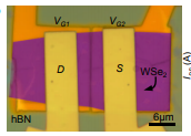
Two dimensional semiconductors have atomically precise widths which leads to strong quantum confinement and large surface areas for direct electrical contacts. In particular, these materials are strongly absorbing due to excitonic resonances arising from strong electron-hole binding energies. Micro-time resolved SWIR fluorescence, and high resolution photocurrent mapping allow us to study how nanomaterial photovoltaics can be achieved through precise electrostatic doping, which minimizes auger recombination of excitons, and maximizes exciton diffusion to the depletion interface.
